Among various nanomaterials, structures with quasi-one-dimensionality (Q1D) have been a research focal point ever since the discovery of carbon nanotube in 1991. Due to the lack of efficient methods to fabricate carbon nanotubes with specific electrical characteristics, tremendous effort has been devoted to the study of semiconducting nanowires with high crystalline structures and controllable physical properties. In the current trend of device miniaturization, these Q1D nanostructures play an important role as the building blocks for devices that could overcome the fundamental limits of microtechnology. Please click to following links to learn more details about different Q1D materials systems we have investigated.
-
Topological insulator (TI) is a crystal which consists of heavy elements such as Bi, Se, Sb, Te, Sn, Pb. In essence, it is an insulator in its bulk, yet it has gapless Dirac cone surface states (similar to graphene), giving rise to surface conduction. The peculiar properties of these surface states stem from the strong spin-orbit coupling within the heavy constituting elements. The conduction in TI materials has another remarkable characteristic, that is, the surface electrons with opposite spins propagate in opposite directions. Furthermore, what makes TI materials extraordinary is that, the spins are locked at right angles to the current flow direction, and the surface states have time-reversal symmetry. Therefore, the surface states are robust and topologically protected against defects and perturbations, leading to reduced scattering and noise suppression.
All these unique properties render topological materials important for both new physics explorations and innovative device applications. Understanding and control of the surface states will lead to enhanced spintronic devices. The presence of topological protection against backscattering ensures dissipationless transport in these materials. In addition, it holds high potential for fault-tolerant quantum computation, as it diminishes the quantum decoherence which is detrimental to stable qubit operation. Furthermore, some TI materials are known to be excellent thermoelectric and phase change materials since they favor similar features, such as heavy elements and small band gaps. Thus, they hold also promises as thermoelectric devices for energy harvest, as well as phase change memory devices.
Nanowires have become an important platform in modern nanoelectronics and photonics for low energy consumption and enhanced device performances. Topological insulator materials in nanowire structure offer an attractive system to study their exotic surface states due to the large surface-to-volume ratio and inherent size confinement. Our project focusses on the topological nature of the surface states in single crystalline TI nanowires, and will investigate the spin texture of their surface states influenced by magnetism and superconductivity. The experimental methods span from synthesis, structure characterization, to charge/spin/thermal transport, angle resolved photoemission spectroscopy, and scanning tunneling spectroscopy measurements.
Low pressure catalytic chemical vapor deposition (CVD) method is used to synthesize single crystalline Sb2Te3 nanowires based on the vapor-liquid-solid growth mechanism. It is a typical CVD system that consists of mass flow control unit, rapid thermal furnace, and vacuum pressure control system. The growth parameters (temperature, pressure and duration) and size of the Au catalyst can be adjusted to obtain nanowires of different diameters and aspect ratios. In the same CVD system, in situ doping can be achieved by introducing dopants in the reaction atmosphere by either thermal heating or pulse laser ablation. Figure 1(b) displays a scanning electron microscopy (SEM) image of a nanowire with rectangular cross section under contact electrode.
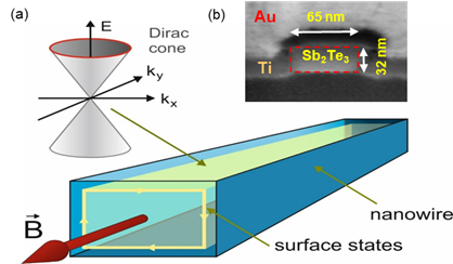
Figure 1 (a) schematic of Sb2Te3 nanowire with rectangular cross section, with linear energy dispersion of surface states. (b) SEM image of cross section of a nanowire contacted by electrode Ti/Au.
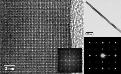
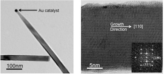
Figure 2(a) shows a typical SEM image of the as-grown Sb2Te3 nanowire and the inset depicts the corresponding energy dispersive spectroscopy (EDS) spectrum, revealing the 2:3 atomic ratio of Sb and Te. Figure 2(b) shows the X-ray diffraction (XRD) spectrum of Sb2Te3 nanowires, verifying the Rhombohedral structure of space group (JCPDS card 00-015-0874). Figure 2(c) shows a high-resolution transmission electron microscopy (HRTEM) image of a single Sb2Te3 nanowire and the inset is the corresponding selected area electron diffraction (SAED), confirming its single crystalline nature and the growth direction along [110].
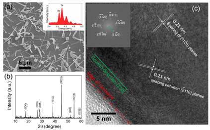
Figure 2 (a) A SEM image of the as-grown Sb2Te3 nanowires. Inset: the corresponding EDS spectrum.
(b) XRD spectrum of Sb2Te3 nanowires. (c) HRTEM image of a single Sb2Te3 nanowire with corresponding SAED as shown in inset.Aharonov–Bohm effect
We have performed a preliminary study on Sb2Te3 nanowires using low temperature magneto-resistance measurements at the Forschungszentrum Jülich. The data pave the way to investigate the fundamental physics of topological insulator nanowires and explore their potential applications. Figure 3 shows magneto-resistance spectra on one nanowire sample contacted with Ti/Au leads with magnetic field applied parallel to the wire axis. The spectra reveal clear mirror symmetry around zero field, as well as periodic oscillation indicated by the dashed lines at the spectra minima. From the data, the dominant flux periodicity around the nanowire is extracted on the order of flux quanta h/e. This demonstrates a clear signature of Aharonov-Bohm type interference, giving evidence of surface conduction.
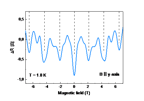
Figure 3 Magneto-resistance spectra in parallel field after subtracting the parabolic background
-
Intrinsic CdS is highly insulating, thus doping is crucial in order to tailor the material property and to control the device functionality. Stable p-type conductivity has shown to be difficult due to the low solubility of the acceptor dopants, deep acceptor levels, and the compensation effect between acceptor dopants and the native donors. In this work, Sn is used as the dopant to explore the self-compensation effect, for Sn is amphoteric to CdS, which yields both donors and acceptors after substitution of either Cd or S. Since the ionic radius of Sn2+ (1.02 Å) is close to that of Cd2+ (0.97 Å), Cd substitution is expected to be more preferential and thus leads to dominating n-type characteristics. The system is comprehensively examined by correlating the optical and electrical properties, via parallel studies in the temperature dependent optical and charge transport measurements.
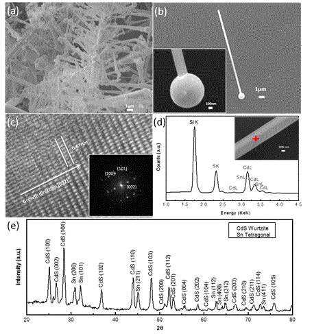
Figure 1 CdS:Sn nanowires are synthesized using catalytic CVD method. Sn serves no only as a catalyst but also a dopant. (a) (a) SEM image of a CdS nanowire ensemble. (b) SEM image of a single nanowire with homogeneous diameter and a round catalyst on the tip. Inset shows an enlarged view of the section near catalyst. (c) HRTEM image of a CdS:Sn nanowire showing single crystalline structure with growth direction along [002] (c-axis). Inset displays a FFT pattern of the HRTEM image. (d) Point EDX spectrum on a single CdS nanowire shows distinct Cd, S peaks. Sn peaks are at the shoulder of the Cd peak. Cd:S:Sn ratio is quantified to be 48.1: 50.2: 1.7. (e) XRD spectrum of a CdS:Sn wire ensemble indicates the wurtzite structure for CdS nanostructures and Sn with tetragonal phase.
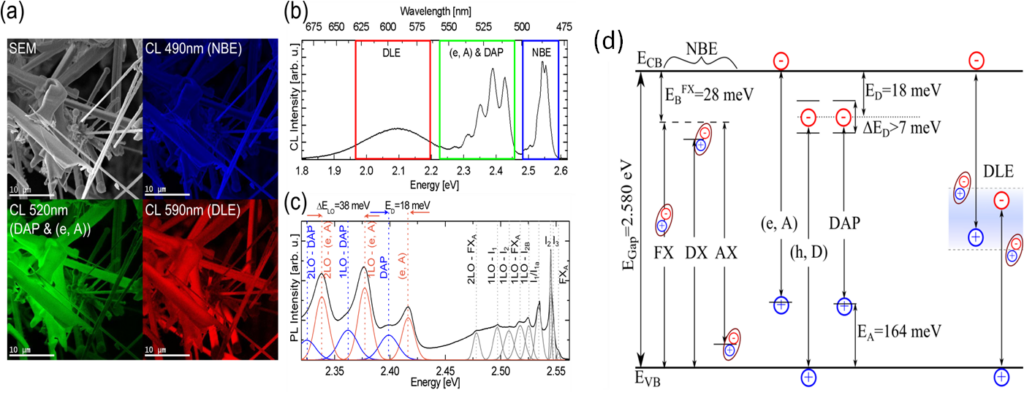
Figure 2 (a) SEM and monochromatic CL images of a CdS:Sn nanowire ensemble. The near band edge emission (NBE) at 490 nm originates mainly from long and straight nanowires, whereas thick structures show predominantly luminescence at 520 nm corresponding to donor-acceptor-pair (DAP) and a free to bound (e, A) transitions. Deep level emission (DLE) centers are homogeneously spread over the ensemble. (b) The low temperature (7 K) CL spectra of the corresponding ensemble in (a) reveals 3 emission regions, NBE (blue), DAP and (e, A) and their LO-phonon replica (green), and the DLE (red). (c) Photoluminescence spectra of CdS:Sn nanowire ensemble, taken at 4 K with a excitation density of 50 mW/cm2 at 325 nm. Several transitions of the NBE are labeled, i.e. the free exciton FXA, donor bound excitons (I2, I3), acceptor bound excitons (I1/I1a), the surface exciton SX, and their phonon replica (ΔELO = 38 meV). The distance between DAP and (e, A) transition corresponds to the binding energy of an electron to a donor ED = 18 meV. (d) The band structure for CdS:Sn nanowires obtained from the optical data shows excitonic transitions: The free exciton FX, donor bound excitons DX and acceptor bound excitons AX, but also non excitonic transitions: free to bound transitions (h, D) and (e, A), or the bound to bound DAP transition. The energies of the transitions result from the band gap EGap=2.58 eV and the corresponding binding energies (EBFX=28 meV,ED=18 meV, EA=164 meV). The deep level defect luminescence appears at energies ranging from 1.8 – 2.2 eV.
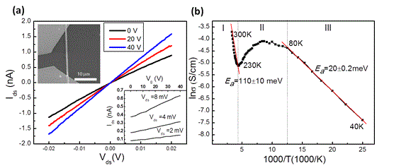
Figure 3 (a) Source–drain current versus voltage of a CdS:Sn single nanowire field effect transistor show good linearity under 0, 20 and 40 V gate voltages. Inset: SEM image of this single wire with Ti/Au contact. Upper left inset: SEM image of single wire FET. Lower right inset: Source-drain current versus gate voltage plots at room temperature under source-drain voltage Vds = 2, 4, and 8 mV, respectively. The transconductance is estimated to be 1.80×10⁻¹² A/V at Vds =2 mV. Carrier concentration n = 8.10×1016 cm-3 and mobility μe = 2.22 cm2/V·s are obtained. (b) Temperature dependence of conductivity depicts the thermal activation of electrons from various donor levels.
-
Single crystalline CdTe nanowires are synthesized using Au-catalyzed chemical vapor deposition. X-ray diffraction reveals the existence of non-negligible inhomogeneous compressive strain in the nanowires along the <111> growth direction. The effect of the strain on the electronic structure is manifested by the blue-shifted and broadened photo-luminescence spectra involving shallow donor/acceptor states. Such residue strain is of great importance for a better understanding of optical and electrical behaviors of various semiconductor nanomaterials as well as for their device design and applications.
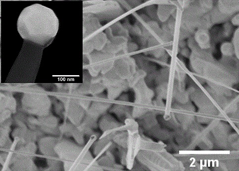
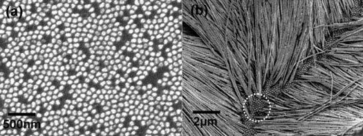
Figure 1 SEM image of as-grown CdTe nanowires.
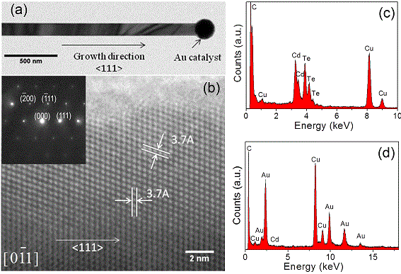
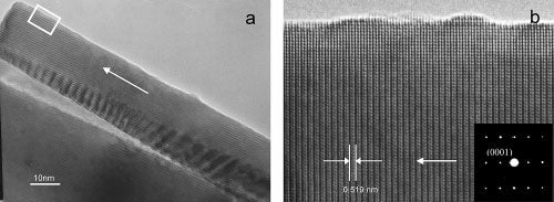
Figure 2 (a) Low magnification of TEM of a CdTe nanowire showing a nanoparticle on the tip of the nanowire (b) HRTEM image shows the growth direction along <111>. Insert: SAED pattern of the HRTEM image. (c) EDS spectrum of CdTe nanowire (d) EDS spectrum of the Au nanoparticle on the tip of CdTe nanowires.
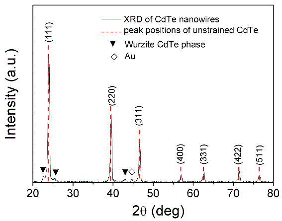
Figure 3 XRD spectrum of CdTe nanowires. Miller indices of the zinc blende CdTe peak are indicated. The peaks labeled by triangle originate from zinc blende CdTe, and the peak labeled with diamond shape originates from Au catalytic particle. The compressive strain along the nanowire axis is determined to be about -1%. And the strain component in the plane perpendicular to the nanowire axis is calculated to be ~ +0.4%.
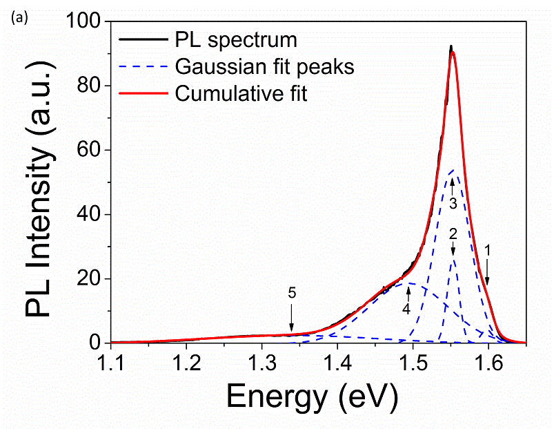
Figure 4 Photoluminesence spectrum of CdTe nanowires measured at 5.0 K. A pronounce blue-shift in the bound exciton peak (Peak #1) was revealed.
-
In recent years magnetic nanostructures have experienced a great interest in dynamic magnetic torque experiments. These experiments explore the possibility to rotate the orientation of the magnetization with a current pulse. This could be an important tool in spintronics. Complementary to the dynamic experiments we want to explore the static properties of magnetic nanostructures, in particular cobalt nanowires (NW). We believe that a detailed knowledge of the static magnetic properties will have important consequences in their dynamic behavior.
-
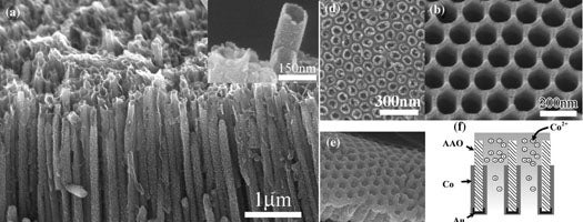
Co nanotube arrays with high filling rate and homogeneous growth have been successfully fabricated by a direct electrodeposition process with low current density. The as-grown nanotubes are predominately of hcp single crystalline structure with the magnetocrystalline easy axis perpendicular to the tube axis. MFM imaging shows a weak magnetic signal and SQUID measurement reveals sheared hysteresis responses for field applied along the tube axis. Combined with theoretical modeling taking into account the shape demagnetization, crystal anisotropy, magnetic exchange, and external magnetic interaction energies, our measurements confirm that the magnetization curls circumferentially around the tube in order to minimize the total magnetic energy for small external fields. Lastly, these magnetic nanotubes with little hysteresis hold promising applications. For example, they may be employed in spintronic devices with reduced hysteresis loss, in magnetic shielding to inhibit field penetration into the center of the tube, and in biomedical applications such as drug delivery and biomolecular separation.
-
-
-
Crystal Structure
As a II-VI compound semiconductor with wide band gap (3.37 eV), zinc oxide (ZnO) has been broadly used in optical applications, for example, optical waveguide, transparent conducting layer, surface acoustic wave device. Recently one-dimensional ZnO nanostructures, such as nanowire, nanoneedle, and nanobelt, are attracting more and more attention. Their optical, mechanical, field emission and magnetic properties have been studied. ZnO nanowire (NW) is expected to be one of the candidates for nanoscale ultra-violet (UV) lasing, light emitting and photodetection. However, electrical transport properties through ZnO NWs have not yet been broadly investigated. Here we report the transport studies on field effect transistors (FET) made of individual ZnO NWs synthesized via chemical vapor deposition (CVD) method. The effects of oxygen adsorption on NW’s electrical behavior are investigated and the oxygen sensing property is characterized. The results indicate that ZnO NWs can serve as potential building blocks for nanoscale electronic and sensing devices.
Single crystal ZnO nanowires doped with indium are synthesized via the laser-assisted chemical vapor deposition method. The conductivity of the nanowires is measured at low temperatures in magnetic fields with directions both perpendicular and parallel to the wire axes. A quantitative fit of our data is obtained, consistent with the theory of a quasi-one-dimensional metallic system with quantum corrections due to weak localization and electron−electron interactions. The anisotropy of the magneto-conductivity agrees with theory. The two quantum corrections are of approximately equal magnitude with respective temperature dependences of T−1/3and T−1/2. The alternative model of quasi-two-dimensional surface conductivity is excluded by the absence of oscillations in the magneto-conductivity in parallel magnetic fields.
Optical Properties
To clarify the size effect in semiconductor nanowires with decreasing diameters but not yet reaching the quantum confinement region, single crystalline zinc oxide nanowires with diameters around 10nm are synthesized. Electrical transport measurements of these thin nanowires show significant increase in conductivity accompanied by diminished gate modulation and reduced mobility. This phenomenon is a result of the enrichment of surface states owing to the increased surface-to-volume ratio. The enhanced surface effect is confirmed by the temperature dependent photoluminescence measurements and contributes to the “anomalous” blueshift. This study shows that surface states play a dominant role in the electrical and optical properties of quasi-one dimensional materials.
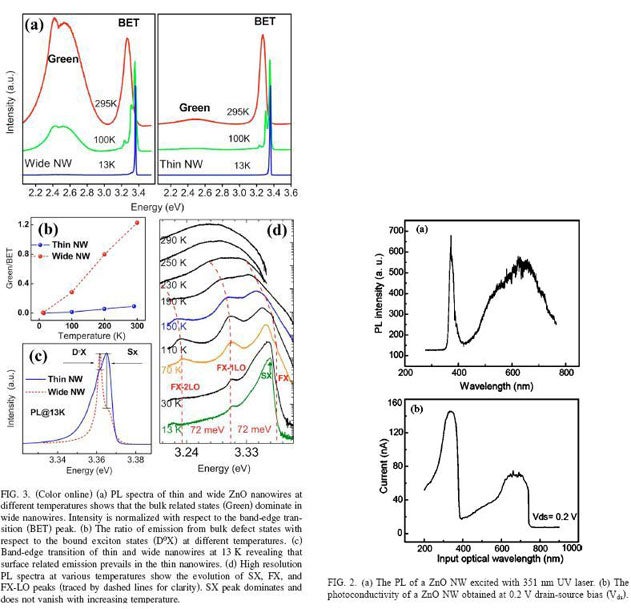
Single crystal ZnO nanowires are synthesized and configured as field-effect transistors. Photoluminescence and photoconductivity measurements show defect-related deep electronic states giving rise to green-red emission and absorption. Photocurrent temporal response shows that current decay time is significantly prolonged in vacuum due to a slower oxygen chemisorption process. The photoconductivity of ZnO nanowires is strongly polarization dependent. Collectively, these results demonstrate that ZnO nanowire is a remarkable optoelectronic material for nanoscale device applications.
Transport Properties
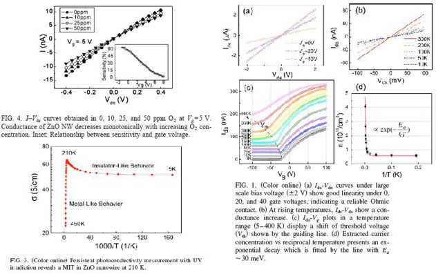
Single-crystal ZnO nanowires are synthesized using a vapor trapping chemical vapor deposition method and configured as field-effect transistors. Electrical transport studies show n-type semiconducting behavior with a carrier concentration of ,~10E7 cm−1 and an electron mobility of ,~17 cm2 /V s. The contact Schottky barrier between the Au/Ni electrode and nanowire is determined from the temperature dependence of the conductance. Thermionic emission is found to dominate the transport mechanism. The effect of oxygen adsorption on electron transport through the nanowires is investigated. The sensitivity to oxygen is demonstrated to be higher with smaller radii nanowires. Moreover, the oxygen detection sensitivity can be modulated by the gate voltage. These results indicate that ZnO holds high potential for nanoscale sensing applications.
Thin ZnO nanowires with diameters of less than 50 nm are configured as field effect transistors and studied for their transport mechanisms at different temperatures under UV illumination and gate modulation. The conductivity exhibits two regimes: at T>50 K, thermally activated transport dominates with activation energy around 30–60 meV attributed to the shallow donor states and at T<50 K, three dimensional variable range hopping reveals in the conduction. In addition, UV irradiation leads to a metal-to-insulator transition at 210 K. Furthermore, electrostatic gating results in a band bending giving rise to a change in the activation energy.
-
Gallium oxide (Ga2O3), a trivalent metal oxide semiconductor, exhibits a wide band gap (4.9eV) and electrically insulating behavior in normal circumstances. Its remarkable thermal and chemical stability renders it suitable for many potential applications. Ga2O3 thin film has been extensively studied and implemented as high temperature oxygen sensor, insulating barrier in spin tunneling junction, and UV-transparent conductive oxide (TCO). In recent years, low dimensional structures have become the rising stars that draw intensive attention because of their unique properties resulted from the high aspect ratio. Quasi-one-dimensional structures of Ga2O3, such as nanowires and nanobelts, have been synthesized and characterized. However, the electrical transport studies on Ga2O3 nanowires demonstrate poor conductivity at room temperature, making it impractical for device applications. With the aim to enhance the charge carrier density, this report describes the synthesis and a p-type doping method. The electrical and optical properties of Ga2O3 nanowires are characterized.
-
Quasi-one-dimensional (Q1D) materials, such as nanotubes and nanowires, are considered as highly promising nanoscale building blocks for integrated electronic and photonic circuits.1,2 In this regard, the control of electron (n-type) and hole (p-type) doping in these nanostructures is of paramount importance.3 The doping approach is usually implemented by incorporating impurity elements during the synthesis procedures.4 In our work, a-Fe2O3 nanobelts are configured as field effect transistors (FETs), followed by a controlled in-situ doping method using zinc (Zn) as the impurity element to achieve p- or enhanced n- type semiconducting property. Carrier concentrations and mobilities are obtained from electrical transport studies. Furthermore, the mechanism of p- and n-type doping using only one impurity element is discussed.