Various techniques have been developed for fabricated Q1D nanostructure, including template assisted and template-free methods. In our lab, we mainly employ two most popular and effective ways: chemical vapor deposition and electrochemical deposition. More details can be found below.
-
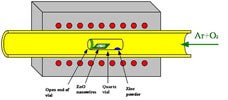
A chemical vapor deposition (CVD) process modified with vapor trapping method has been used to synthesize n-type ZnO nanowires with high carrier concentration without incorporating impurity dopants. With this method, a spatial variation of synthesis condition was created and the donors were directly introduced into the nanowires during the synthesis process. Electron microscopy and electrical transport studies show that nanowires having distinct morphologies and electrical properties were obtained at different locations in the CVD system. The vapor trapping method elucidates the effect of synthesis conditions, and provides an approach to control nanowire growth for tailorable device applications.
-
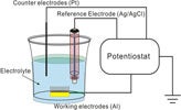
Antimony nanowires with a high aspect ratio were produced by pulsed electrodeposition in a template of a porous anodic aluminum oxide (AAO) membrane . The fabrication procedures of vertically oriented Sb nanowire arrays are made. In the first step, a bilayer metal thin film, Ti/Au (20/300 nm), is patterned onto the AAO membrane as the bottom electrode. In the second step, the AAO template is submersed into a three-electrode electrolytic cell, with the bottom Ti/Au electrode serving as the working electrode. Subsequently, a wet etching process is carried out to partially remove the AAO template and to expose the Sb nanowire arrays. A thin layer of AAO is intentionally left to serve as an isolation layer at the interface between the liquid analyte and the bottom electrode contact. To further control the number ofexposed nanowires, photolithography can be utilized to define the position of the nanowire electrodes, and therefore to control the electrode density.The acid and base properties of electrolytes in living cells play an important role in any biological process, as the pH value is the most critical parameter in chemical and biochemical reactions. Conventionally, pH meters use glass tube-based pH electrodes for measuring the H+ concentration in tested samples containing a sufficient amount of aqueous electrolyte. Those glass electrodes are inappropriate for use in miniaturized and real-time monitoring devices. With the increasing demand of portable biomedical sensing devices, it is crucial to find a solution to make nano/biointegrated sensors for precise pH determination. In the following, we demonstrate that the Sb nanowire functions as a reliable solid-state pH sensor. Before performing pH measurements, a set of standard solutions was prepared with a 0.02m Tris buffer solution and the H+ concentration was adjusted by adding a proper amount of 3m NaOH and/or HCl. A commercial Accumet AB-15 pH meter was used to calibrate a series of standard solution with pH values from 2 to 12. The pH value was determined at room temperature by potentiometric measurement according to the potential difference between the reference electrode and the Sb nanowire electrode.
Templates for electrochemical deposition
-
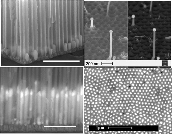
Anodic aluminum oxide (AAO) membrane that consists of hexagonally ordered nanopores has been the most commonly used template for fabricating semiconductor nanowire arrays because of its chemical stability, insulating characteristics and good mechanical strength. More importantly, morphologies of AAO (pore size, pore-to-pore distance and channel length) can be readily adjusted by anodization parameters, allowing a convenient way for obtaining controllable nanowire structures. Therefore, it provides an easy way to fabricate nanowires with sizes within the quantum confinement region ( < 10 nm in diameter).
-
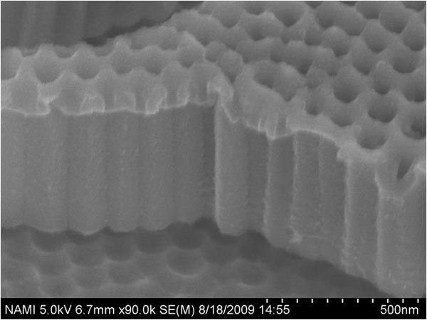
Highly ordered anodic titanium oxide nanotubes film has been synthesized by two-step anodization. By using a reductive doping method, the guest materials (Cu and Ni) are electrodeposited into the nanotubes benefited from the improved conductivity at the tubes bottom. The versatile process yields reproducible tubular structures in ATO nanotubes due to the conductive nature of crystallized TiO2. Dye-sensitized solar cells have also been demonstrated by employing the ATO films. It is observed that bottom treatment induces greatly enhanced short current density and fill fact, resulting in an improved energy conversion efficiency of 3.9 %. The enhanced photovoltaic performance could be attributed from the increased conductivity at the tubes bottom accompanied with the reduction of the series resistance.