Due to their excellent electrical, optical and piezoelectric properties, Q1D nanostructures offer a wealth of device applications. Some of the devices application are investigated as detailed below:
Electronic Devices
-
We have recently observed for the first time a non-local spin valve signal in a TI (Sb2Te3) channel as illustrated in Figure 1. The Sb2Te3 nanowires were dispersed onto a thermally oxidized Si substrate. Individual nanowires were located and registered via SEM imaging, and two levels of aligned e-beam lithography were used to pattern non-magnetic outer Au leads and two magnetic tunnel junction AlOx/Py/Cu/Co inner leads. The tunnel junction leads consist of a free Py (Ni80Fe20) layer, whose magnetization determines the magnitude and direction of spin current injected into the Sb2Te3 nanowire. The partially oxidized Co layer merely serves as a pinned reference layer (exchange biased by CoO) that allows us to unambiguously determine the direction of the Py layer magnetization via measuring current-in-plane magneto-resistance of the lead itself.
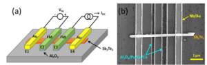
Figure 1 (a) Schematic of the nonlocal spin valve device based on a TI Sb2Te3 nanowire channel. (b) SEM image of the device. Py/Cu/Co/CoO composite spin valve electrodes with a pinned Co/CoO reference layer are employed to unambiguously determine the Py injector magnetization direction in each of the magnetic electrodes.
Measurements of the device resistance between the two Au leads reveal that the Au/Sb2Te3 contact is ohmic (low resistance, linear I-V characteristic). The two-point resistance measured between these contacts as a function of magnetic field shown in Figure 2 exhibits positive magneto-resistance. This positive magneto-resistance originates from weak anti-localization of carriers in the Sb2Te3 nanowire induced by spin-orbit interaction. The weak anti-localization signal serves as evidence of a strong impact of spin orbit interaction on transport in the Sb2Te3 nanowire system.
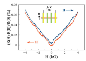
Figure 2: Positive magneto-resistance of the Sb2Te3 nanowire arising from weak anti-localization of carriers in the nanowire induced by spin-orbit interactions. Inset illustrates the applied magnetic field direction as well as the two-point measurement geometry employed.
-
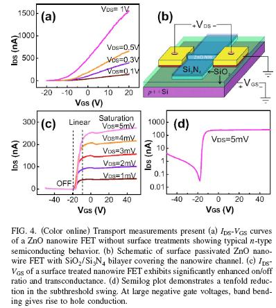
ZnO nanowires with high crystalline and optical properties are characterized, showing strong effect of the surface defect states. In order to optimize the performance of devices based on these nanowires, a series of complementary metal-oxide semiconductor compatible surface passivation procedures is employed. Electrical transport measurements demonstrate significantly reduced subthreshold swing, high on/off ratio, and unprecedented field effect mobility.
-
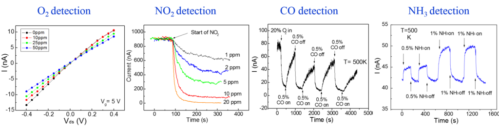
Zinc oxide nanowires were configured as n-channel field-effect transistors. These transistors were implemented as chemical sensors for detection of various gases. Nanowire’s ammonia sensing behavior was observed to switch from oxidizing to reducing when temperature increased from 300 to 500 K. This effect is attributed to the temperature dependent chemical potential shift. Carbon monoxide was found to increase the nanowire conductance in the presence of oxygen. In addition, nanowire detection sensitivity dependence on the diameter was investigated.
ZnO nanowire field effect transistors were implemented as highly sensitive chemical sensors for detection of NO2 and NH3 at room temperature. Due to a Debye screening length comparable to the nanowire diameter, the electric field applied over the back gate electrode was found to significantly affect the sensitivity as it modulates the carrier concentration. A strong negative field was utilized to refresh the sensors by an electrodesorption mechanism. In addition, different chemisorbed species could be distinguished from the “refresh” threshold voltage and the temporal response of the conductance. These results demonstrated a refreshable field effect sensor with a potential gas
identification function.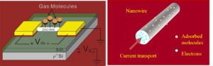
-
Antimony (Sb) has a remarkable linear response to the H+ concentration in solution and it is applied for commercial pH electrodes.Unlike conventional glass tube-based pH electrode, the solid-state Sb electrode represents a good candidate for an integrated pH sensor with a fabrication process that is compatible to the silicon-based complementary metal oxide semiconductor (CMOS) process. In addition, due to its high resistance to corrosion, the Sb-based pH electrode has been used in a wide range of applications. For instance, the Sb electrode withstands hydrofluoric (HF) acid and allows reliable determination of the proton concentration in HF-containing solution in which a glass electrode normally cannot be used. Moreover, the Sb electrode has demonstrated effectiveness in clinical operations. It has been utilized to determine the intramyocardial pH during open-heart surgery, the ambulatory esophageal pH, and dental plaque pH. In addition, by coating with suitable enzymes, the Sb electrode functions as a potentiometric enzyme electrode that can be used to determine the concentration of urea. Because of its versatile sensing applications, the Sb probe with a size scale that is compatible to cells has great potential for meeting the demands of biomedical research.The in vivo and in vitro intracellular real time monitoring of pH, Na+, K+—a key subject in cell biology and physiology—may require vertically oriented nanoscale electrodes in close contact with cells. Such nanoelectrodes can be implemented by vertically grown nanowires and they can be applied to penetrate smoothly and gently into a cell without causing cell apoptosis. Herein, we describe a method for fabrication of vertical Sb nanowire electrodes, present their property characterization and demonstrate their potential application for pH sensing.
-
For decades, electronic devices have been relying on the transport of electronic charge. The electron spin degree of freedom, however, was often ignored. A new technology called spin electronics (Spintronics) has emerged since the discovery of giant magnetoresistance (GMR) effect in 1988. Today, GMR read head has become the key for high-density magnetic information storage. At the same time, much progress has been made in making magnetic random access memory (MRAM) based on the tunneling magnetoresistance (TMR) effect. The ability to manipulate electron spin states is critical to extremely high-density information storage, electron-spin-based quantum computing, magneto-electronic sensors, and perhaps future spin electronic devices and systems yet to be imagined. As the trend of device miniaturization continues, such applications require a good understanding of the fundamental physics of spin dependent transport in nanoscale structures.
The proposed project is to combine the recent developments in spin tunnel junctions and single electron transistors, to fabricate and characterize nanoscale hybrid junction structures that reveal new physical aspects of quantum states and dynamic behavior of single electron spins. Several interesting effects have been predicted for spin-dependent transport in ferromagnet (FM)/metal/FM and FM/superconductor/FM single electron transistors. The project is aimed to experimentally verify these theoretical predictions. The approach of this study is to fabricate hybrid junction devices using ebeam lithography and shadow evaporation techniques. This work contributes to the current research in spintronics community and provides more comprehensive understanding of the spin dynamics in order to develop innovative spin based nanoelectronic devices.
Energy Devices
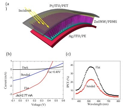
ZnO nanowire flexible dye sensitive solar cell
-
Highly ordered anodic titanium oxide nanotubes film has been synthesized by two-step anodization. By using a reductive doping method, the guest materials (Cu and Ni) are electrodeposited into the nanotubes benefited from the improved conductivity at the tubes bottom. The versatile process yields reproducible tubular structures in ATO nanotubes due to the conductive nature of crystallized TiO2. Dye-sensitized solar cells have also been demonstrated by employing the ATO films. It is observed that bottom treatment induces greatly enhanced short current density and fill fact, resulting in an improved energy conversion efficiency of 3.9 %. The enhanced photovoltaic performance could be attributed from the increased conductivity at the tubes bottom accompanied with the reduction of the series resistance.
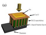
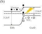
Anodic titanium oxide nanotubes film has been synthesized by two-step anodization. The conductivity at the crystallized barrier layer can be improved by NH4Cl treatment, which facilitates the high filling rate electrodeposition. Three dimensional Cu2O/TiO2 p-n junction arrays are then constructed by electrodepositing Cu2O into TiO2 nanotube matrix. The improved photovoltaic performances benefits from the high junction interface as well as the quasi-one-dimensional carriers’ pathway due to the radial hetero-junction nature. The versatile process can be used to fill various metal or semiconductor for functional applications.
-
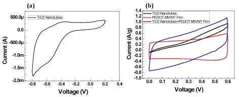
Highly conducting and porous carbon nanotubes are widely used as electrode in double-layer-effect supercapacitors. In this presentation, vertical TiO2 nanotube arrays are fabricated by anodization process and used as supercapacitor electrode utilizing its compact density, high surface area and porous structure. By spin coating carbon nanotube networks on vertical TiO2 nanotube arrays as electrodes with 1M H2SO4 electrolyte in between, the specific capacitance can be enhanced by about 30% compared to using pure carbon nanotube network alone because of the combination of double layer effect and redox reaction from metal oxide materials. With cyclic voltammetry (CV) and galvanostatic (GV) charge-discharge measurements, this type of hybrid electrode has proven to be suitable for high performance supercapacitor application. The electrochemical impedance spectroscopy technique shows that the device has good capacitive behavior and electrical conductivity. This approach is also a potential application for flexible electronics.